Click here for a higher resolution (larger) schematic.
Introduction:
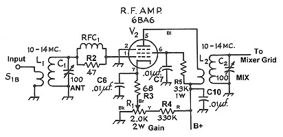
The RF amplifier takes the signal from the antenna and amplifies it by an
amount determined by the setting of the RF gain control. Signal levels can vary
over a very wide range. With very strong signals, the RF amplifier may not even
be needed, but for weak QRP signals a substantial amount of gain is required.
To handle this wide range of signal levels, the RF amplifier gain must be
smoothly adjustable over an equally wide range.
In audio amplifiers, simple voltage dividers (potentiometers or "volume
controls") are used to control the gain, but these can't be used at RF
because of capacitive leakage around them. For RF voltage amplifiers, the usual
method is to use a vacuum tube known as a remote cutoff pentode. The gain of
such a tube is controlled by varying the grid bias on the tube. More advanced
circuits automatically control the grid bias to provide automatic gain control
(AGC) but in the 6x2C converter the gain is controlled manually. In many cases
this is actually an advantage.
Though there are many tubes suitable as RF amplifiers, I chose to use the 6BA6.
I used the 6BA6 as the
IF amplifier
circuit in the 6x2 receiver and found it worked very well. Since that
circuit worked so well, I chose to use it here, not as an IF amplifier but as
an RF amplifier. This circuit is essentially the same as the
IF amplifier
circuit in the 6x2 receiver, but with different input/output coupling. The
RF gain control varies the bias on the tube so that the gain can be changed by
approximately 20 db from minimum to maximum. There is plenty of gain for even
the weakest of signals, but the gain can be easily reduced to handle stronger
signals.
RF Amplifier
Circuit
Click On Any Part Of The Schematic Diagram Below For
Information On That Part Of The Circuit
Click On Any Part Of The Schematic Diagram Above For
Information On That Part Of The Circuit
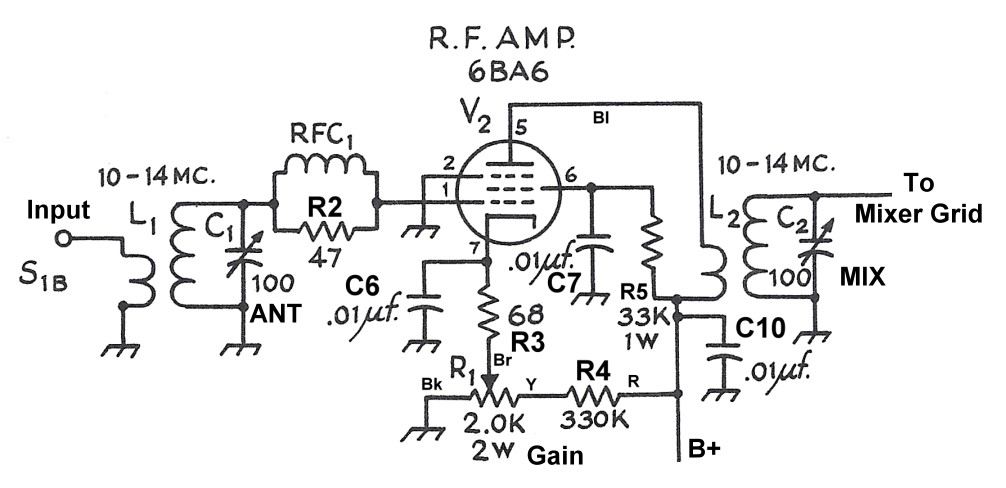
| Input From Antenna: Input to the RF amplifier is via a 3 turn link on L1. The secondary of L1 and ANT control C1 form a parallel resonant circuit. The ANT control resonates this circuit at either 30m or 20m. This resonant circuit is connected to the grid of the 6BA6 tube via a parasitic suppressor. |
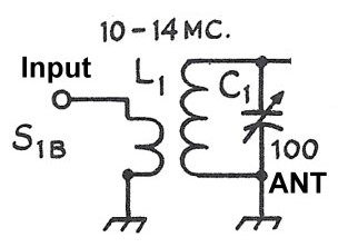 |
| Parasitic Suppressor: The RF amplifier is capable of high gain. To prevented unwanted parasitics, a parasitic suppressor is placed between the input from the antenna and the grid of the 6BA6. |
 |
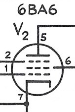
| 6BA6 Vacuum Tube: The 6BA6 vacuum tube is a remote cutoff pentode. By varying the bias on the tube with the RF Gain Control the gain can be smoothly controlled. The 12V version of the 6BA6, the 12BA6, was used in the popular "`All American Five" AM receivers. You can click on this link for a 6BA6 data sheet. |
 |
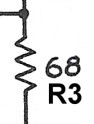
| Cathode Bias Resistor: The 68 ohm cathode resistor provides for a minimum bias on the tube and controls the maximum gain of the stage. The voltage drop developed across this resistor and the RF gain control is the operating bias on the tube. When the GAIN control is set for maximum gain (fully CW), only the 68 ohm resistor is in the circuit, the bias is a minimum, and the gain is a maximum. |
 |
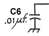
| Cathode Bypass Capacitor: The cathode must be kept at ground potential for RF, otherwise the gain of the tube will be reduced due to negative feedback. The cathode bypass capacitor shunts RF around the cathode bias resistor and RF gain control keeping the cathode at ground potential for RF. |
 |
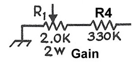
| RF Gain Control And Dropping Resistor: Effective gain control is important in the converter. The gain must be variable to permit reception of weak signals, yet prevent overload on strong signals. In the 6x2C, a remote cutoff pentode, the 6BA6, is used in the RF stage. The gain of a remote cutoff pentode is controlled by the bias on the tube. Higher bias reduces the gain of the tube. The GAIN control and dropping resistor are used to control the bias on the tube. Maximum gain is controlled by the 68 ohm cathode bias resistor. When the GAIN control is fully clockwise, the wiper is at the grounded end of the control and only the 68 ohm cathode bias resistor is in the circuit. This produces minimum bias, and maximum gain. When the control is fully CCW, the wiper is at the end connected to the 330k resistor. Current through the tube and the 330k resistor then passes through the GAIN control resistance, developing a much larger voltage drop, maximizing the bias. This reduces the gain to a minimum. The 330k resistor controls the minimum gain. Without the 330k resistor, the maximum voltage drop across the GAIN control would be insufficient to reduce the gain to the desired amount. The 330k resistor increases the maximum voltage drop across the IF gain control resistance. Decreasing the value of the 330k increases the maximum voltage drop, lowering the minimum gain. Increasing the value of the 330k resistor decreases the maximum voltage drop, increasing the minimum gain. |
 |
| B+ Plate Supply: The RF amplifier is powered from the B+ supply, which is nominally 122V. |
 |
 Back to Dr.
Greg Latta's Electrical Engineering and Amateur Radio Pages
Back to Dr.
Greg Latta's Electrical Engineering and Amateur Radio Pages
 If you have any questions or
comments, you can send E-Mail to Dr. Greg Latta at
glatta@frostburg.edu
If you have any questions or
comments, you can send E-Mail to Dr. Greg Latta at
glatta@frostburg.edu