Click here for a higher resolution (larger) schematic.
Introduction:
When the internal VFO is used it must be amplified before reaching the
buffer/multiplier stage. When the Crystal/VFO switch is set to the VFO or ZERO
position the crystal oscillator/buffer stage is configured as a buffer
amplifier by disconnecting the grid coupling capacitor and shorting out the
cathode RF choke and cathode feedback capacitor. In the schematic diagrams
on this page, it is assumed that the Crystal/VFO switch is in the VFO or ZERO
position.
Buffer
Circuit
Click On A Section of the Schematic
Below for Information on That Part of the Circuit:
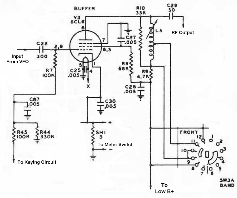
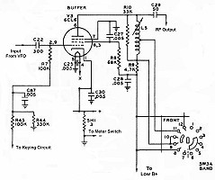
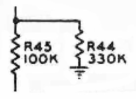
| Keying Resistors: Grid block keying is used in the Johnson Viking Ranger. While the key is up the keying circuit applies a negative voltage across resistors R45 and R44 which function as a voltage divider, and also isolate the buffer somewhat from the output of the keying circuit. About 3/4 of the applied voltage is passed on through the grid leak resistor to the grid of the tube, shutting it off. When the key is pressed, the blocking voltage is removed and the circuit begins amplifying. |
 |
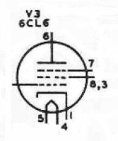
| 6CL6 Tube: In 1950, an important article in QST magazine, "Crystal-Controlled Oscillators, A Review of Modern Crystals, Circuits and Tubes" (QST, March 1950, C. Vernon Chambers, W1JEQ) addressed several points concerning crystal oscillators, including which tube to use. In that article, various electron-coupled circuits were tried along with a variety of tubes: the 6AG7, 6F6, 6V6GT, and 6L6. Among the many conclusions in the article, one came through loud and clear, which I quote here: "Of the four tubes tested the 6AG7 is by far the best from every standpoint." As a result of that article, virtually all crystal oscillator circuits in the ARRL handbook for the next 15 years featured or recommended the use of the 6AG7. The 6CL6 is the 9-pin miniature equivalent of the 6AG7, so it will give exactly the same performance as the 6AG7 in a smaller package. You can click here for a 6CL6 data sheet. Though the 6CL6 was selected for its performance as a crystal oscillator, it also functions very well as a buffer amplifier. |
|
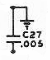
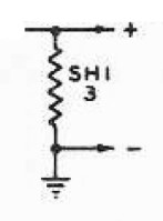
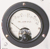
| Meter Bypass Capacitor: The meter bypass capacitor prevents any RF that may be present from getting through to the front panel meter, causing erroneous readings. |
 |
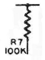
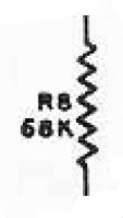
| Output Tank Circuit: The output of V3 is fed to a tank circuit controlled by the band switch. The bandswitch switches in and out R9 and various portions of L5, the tank coil. Resistor R10 loads the tank coil and lowers the overall Q of the circuit. The effect is to select the proper output frequency without requiring an additional tuning control on the front of the transmitter. |
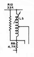 |
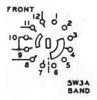
| Band Switch: The band switch shorts out various resistors and coil sections in the output tank circuit to select the correct output frequency from the oscillator and to keep the output as uniform as possible. |
|
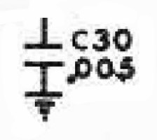
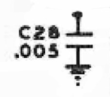
| Plate Bypass Capacitor: The plate bypass capacitor grounds the bottom of the output tank circuit for RF while blocking the DC plate voltage on the tube. It also prevents any RF from reaching the low B+ supply. |
 |
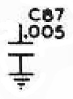
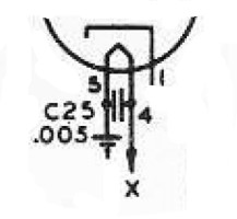
| Filament Bypass Capacitor: When used as a crystal oscillator , the cathode of the 6CL6 is not grounded for RF. Even though there is no direct connection between the filament and the cathode, there is a capacitive connection, and it is possible for RF to get on the filament through the filament/cathode capacitance. Filament bypass capacitor C25 shorts any of this residual RF to ground making sure that none of it escapes. |
 |
 Back to Dr.
Greg Latta's Electrical Engineering and Amateur Radio Pages
Back to Dr.
Greg Latta's Electrical Engineering and Amateur Radio Pages
 If you have any questions or
comments, you can send E-Mail to Dr. Greg Latta at
glatta@frostburg.edu
If you have any questions or
comments, you can send E-Mail to Dr. Greg Latta at
glatta@frostburg.edu