Click here for a higher resolution (larger) schematic.
Introduction:
The buffer/multiplier stage in the Johnson Viking Ranger functions as a buffer
amplifier to raise the level of the signal so that the final amplifier can be
properly driven. A better name for the buffer/multiplier might be
"driver", since it drives the final amplifier stage.
The operation of the buffer/multiplier is very similar to that of the crystal
oscillator/buffer stage when that stage
is used as a buffer. The primary difference is that the output tuning and
gain of the buffer/multiplier stage are controlled by the operator from the
front panel with the "Buffer" and "Drive" controls. This
way the proper drive (as indicated by final amplifier grid current) for the
final amplifier stage can be obtained.
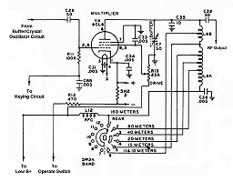
Multiplier
Circuit
Click On A Section of the Schematic
Below for Information on That Part of the Circuit:
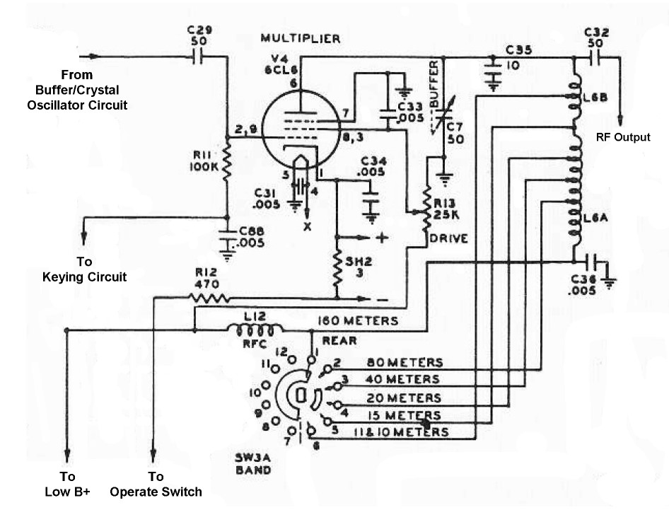
| Keying Circuit: Grid block keying is used in the Johnson Viking Ranger. While the key is up the keying circuit applies a negative voltage togrid leak resistor R11. The voltage passes through the resistor to the grid of the tube, shutting it off. When the key is pressed, the blocking voltage is removed and the circuit begins amplifying. |
 |
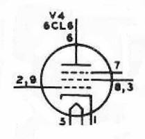
| 6CL6 Tube: In 1950, an important article in QST magazine, "Crystal-Controlled Oscillators, A Review of Modern Crystals, Circuits and Tubes" (QST, March 1950, C. Vernon Chambers, W1JEQ) addressed several points concerning crystal oscillators, including which tube to use. In that article, various electron-coupled circuits were tried along with a variety of tubes: the 6AG7, 6F6, 6V6GT, and 6L6. Among the many conclusions in the article, one came through loud and clear, which I quote here: "Of the four tubes tested the 6AG7 is by far the best from every standpoint." As a result of that article, virtually all crystal oscillator circuits in the ARRL handbook for the next 15 years featured or recommended the use of the 6AG7. The 6CL6 is the 9-pin miniature equivalent of the 6AG7, so it will give exactly the same performance as the 6AG7 in a smaller package. You can click here for a 6CL6 data sheet. Though the 6CL6 was selected for its performance as a crystal oscillator, it also functions very well as a buffer amplifier or multiplier. |
 |
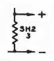
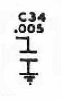
| Cathode Bypass Capacitor: Cathode bypass capacitor C34 shunts any RF around the metering resistor SH2and cathode bias resistor R12 to ground. It is particularly important that no RF flows through the cathode bias resistor as this would result in negative feedback and reduce the gain of the stage. |
 |
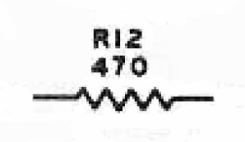
| Cathode Bias Resistor: If bias for the buffer/multiplier stage is provided only by grid leak bias from grid leak resistor R11, the bias on the tube will drop to zero if excitation is lost. Without another source of bias, the tube current will be excessive and the tube will be damaged. By placing resistor R12 in series with the cathode to provide additional bias, the voltage drop across R12 will bias the tube and protect the tube from excessive current in the event of excitation failure.. (In other stages such as the crystal oscillator/buffer the DC resistance of the cathode RF choke serves the same purpose.) |
 |
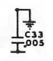
| Screen Bypass Capacitor: The screen grid of the tube must be kept at ground potential for RF. The screen bypass capacitor C33 short circuits any RF on the screen grid to ground while preventing the screen DC supply from being short circuited. |
 |
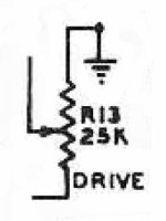
| Screen Drive Control: The gain of the buffer/multiplier must somehow be controlled so that the proper drive can be applied to the final amplifier. The best way to control the gain is by varying the screen voltage on the buffer/multiplier tube. "Drive" control R13 functions as an adjustable voltage divider connected between the low B+ supply and ground. Rotating the control clockwise increases the screen voltage and thus the gain of the buffer/multiplier stage. |
 |
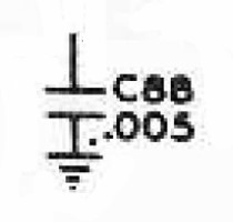
| Multiplier Tank Circuit: The output of V4 is fed to a tank circuit tuned by the "Buffer" control C7 on the front panel. Capacitor C35 provides additional capacitance so the circuit will resonate on the 160m band. The band switch adds and removes inductance so that the circuit will resonate at the proper frequency. Plate bypass capacitor C36 grounds the bottom of the tank circuit for RF. |
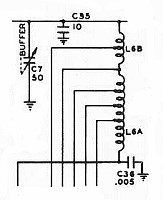 |
| Plate Bypass Capacitor: The plate bypass capacitor C36 grounds the bottom of the output tank circuit for RF while blocking the DC plate voltage on the tube. In conjunction with the plate RF choke L12 it also helps to prevent any RF from reaching the low B+ supply. |
 |
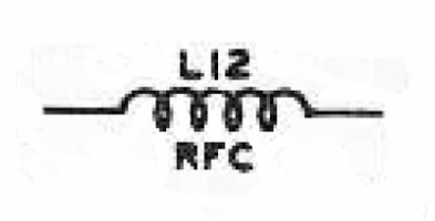
| Plate RF Choke: The plate RF choke prevents any RF from getting back into the low B+ supply while allowing the DC current to reach the plate of the buffer/multiplier tube. |
 |
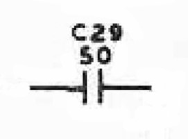
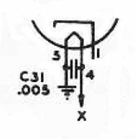
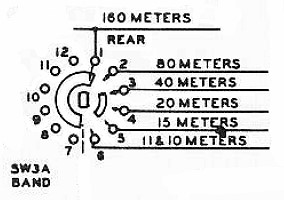
| Band Switch: The band switch progressively shorts out tank coil L6 as the switch is rotated clockwise, decreasing the inductance of L6, raising the resonant frequency of the circuit.. |
 |
| Plate Coupling Capacitor: RF appearing at the plate must be fed to the next stage for amplification. However, the DC plate voltage must not be allowed to pass through to the next stage. The plate coupling capacitor C32 allows the RF to pass through while blocking the DC. |
 |
 Back to Dr.
Greg Latta's Electrical Engineering and Amateur Radio Pages
Back to Dr.
Greg Latta's Electrical Engineering and Amateur Radio Pages
 If you have any questions or
comments, you can send E-Mail to Dr. Greg Latta at
glatta@frostburg.edu
If you have any questions or
comments, you can send E-Mail to Dr. Greg Latta at
glatta@frostburg.edu