Click On Any Section of the Schematic
Below for Information on That Part of the Circuit:
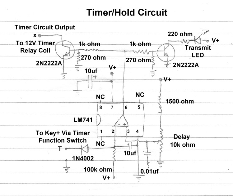
Timer/Hold Circuit:
Note: The timer circuit must be connected across a key connected to a
positive keyed transmitter. Connecting it across a negative keyed
transmitter will damage the circuit.
Whenever the Key+ input is grounded, the circuit goes into transmit mode,
turning on both output transistors, and thus the
12V timer relay and the
transmit LED. As long as the operator keeps sending, the circuit stays in
transmit mode. When the operator stops sending, the circuit stays in transmit
for a hold time controlled by the delay control, and then goes back into
receive mode.
Timer/Hold Circuit
Click On Any Section of the Schematic
Below for Information on That Part of the Circuit:
Operation:
The 2N2222A output transistors are controlled by the LM741 operational
amplifier (op amp), which is configured as a comparator. When the output of the
op amp is low, the transistors are turned off and the unit is in receive mode.
When the op amp output is high, the transistors are turned on, activating the
timer relay and transmit LED. The unit is then in transmit mode.
The operation of an op amp as a comparator is simple. If the - input (pin 2) is
lower than the + input (pin3), then the op amp is turned on and the output
rises to the supply voltage. If the - input is higher than the + input, then
the op amp is turned off, and the output drops to zero.
The 1500 ohm resistor and the 10k ohm delay control function as a voltage
divider, placing an adjustable constant positive voltage on the + input of the
op amp. The combination limits the maximum voltage on the + input to 87% of the
V+ supply voltage. In receive, when the key is up, the 10uf timing capacitor
between the - input and ground charges up through the 100k ohm timing resistor
to 100% of the the supply voltage V+. Since the + input is always limited to a
maximum of 87% of V+, the - input in receive mode is higher than the +
input, and the op amp is turned off.
Whenever the key is pressed, the 10uf capacitor is discharged, and the - input
is brought to ground. Since it is now lower than the + input, the op amp
turns on, and the unit goes into transmit mode. When the key is lifted, the
capacitor starts to charge up again. The rate at which the capacitor charges is
controlled by the 100k ohm timing resistor. The rate is slow enough that during
keying the capacitor never has a chance to charge up enough to reach the
voltage set by the delay control on the + input, and the unit remains in the
transmit mode. However, when the operator stops sending, the voltage across the
capacitor (and the - input) reaches and exceeds the voltage on the + input,
shutting off the op amp and putting the unit back in receive mode. The higher
the voltage set on the + input by the delay control, the longer it takes for
this to happen, and the longer the hold time.
2N2222A Output Transistors:
The output transistors are simple switching transistors. I used 2N2222A
transistors, though just about any NPN transistor, such as a 2N3904, should
also work here. The left transistor controls the timer relay, and the right
transistor controls the transmit LED.
1k Ohm and 270 Ohm Transistor Voltage
Divider Resistors:
The output of the op amp is too high to apply directly to the base of the
output transistors. The 1k ohm and 270 ohm resistors form a voltage divider
that drops the output voltage of the op amp down to a proper value to drive the
output transistors.
10uf Power Supply Bypass Capacitor:
The power supply bypass capacitor provides additional filtering of the V+ power
supply and decouples the timer circuit from the rest of the T/R system.
V+ Power Supply:
Information on the V+ power supply can be found on the
power supply page.
LM741 Operational Amplifier/Comparator:
The 741 is a very popular operational amplifier. Just about any operational
amplifier could be used here, with appropriate changes to the connections. In
this circuit the operational amplifier is used as a comparator. The operation
of an op amp as a comparator is simple. If the - input is lower than the +
input , then the op amp is turned on, and the output rises to the supply
voltage. If the - input is higher than the + input, then the op amp is turned
off, and the output drops to zero..
Transmit LED:
The transmit LED provides a visual indication that the system is in the
transmit mode.
100k Ohm Resistor and 10uf Capacitor -
Timer Components:
The 100k ohm resistor and 10uf capacitor determine how quickly the voltage on
pin 2 rises each time the key is opened. They are adjusted to keep the unit in
transmit mode while the operator is sending, and to provide adequate hold time
after the operator stops sending.
1500 Ohm Resistor, 10k Delay Control, and
0.01uf Capacitor - Delay/Comparator Voltage Divider and Capacitor:
The 1500 ohm resistor and delay control form a voltage divider that applies a
constant adjustable voltage to the + input of the op amp. The 1500 ohm resistor
limits the maximum voltage that can be applied to the + input to 87% of V+.
This guarantees that the system will go back into receive mode when the
operator stops sending even if the delay control is turned all the way up. The
0.01uf capacitor filters out any noise from the wiper of the delay control to
prevent erratic tripping of the timer.
1N4002 Keying Diode:
The keying diode prevents the positive voltage on the key from charging the
timer capacitor, while allowing the capacitor to discharge when the key is
pressed.
 Back to Dr. Greg Latta's
Electrical Engineering and Amateur Radio Pages
Back to Dr. Greg Latta's
Electrical Engineering and Amateur Radio Pages
 If you have any questions or
comments, you can send E-Mail to Dr. Greg Latta at
glatta@frostburg.edu
If you have any questions or
comments, you can send E-Mail to Dr. Greg Latta at
glatta@frostburg.edu