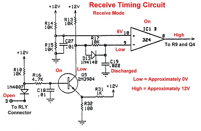
Receive Timing Circuit in Receive Mode
| Main Page | Handshake Circuit |
| How PIN Diodes and PIN Diode Switches Work | QSK Indicator Modification |
| Building an Electronic Transmit/Receive Switch Using PIN Diode Switches | Hot Switching |
| PIN Switch Driver - Turning A PIN Diode Switch Off and On | Circuit Board And Parts Identification |
| T/R Input and Timing Circuits | Schematic Diagram and Circuit Descriptions |
Safety Note: Working on or testing the QSK-5 and associated circuitry may involve operating the amplifier containing the QSK-5 with the cover off. This is extremely dangerous since very high voltages are present when the amplifier is turned on, sometimes in close proximity to the QSK-5. If at all possible, do all work with the amplifier off and unplugged. The operator assumes all risk and liability in such matters! Never operate the amplifier with the cover off unless you are experienced with working around very high voltages!
| Important Timing Considerations |
| Receive Mode |
| Receive to Transmit Transition |
| Transmit Mode |
| Transmit to Receive Transition |
| Transmit Timing Circuit |
Important Timing Considerations:
When a mechanical relay is used for transmit/receive switching in an amplifier,
the physical construction of the relay prevents the output of the amplifier
from ever being simultaneously connected to the input of the amplifier.
However, when an electronic T/R switch
is used, it is quite possible to turn on both the transmit and receive
switches at the same time. If this happens the results will be catastrophic. If
the output of the amplifier is connected to the input for even the tiniest
length of time, the amplifier will become a high powered oscillator that is
connected to the antenna and the transmitter/transceiver output, resulting in
damage to the transmitter/transceiver, amplifier, and/or electronic T/R switch.
Thus, the electronic transmit and receive switches must never be
on at the same time!
The first step in guaranteeing that the transmit and receive switches are never
on at the same time is to design the control circuits so that when one
switch is on the other is always always off. However, because PIN
Switches can be partially on or off, it is possible, if both switches
are activated at the same time, for both to be partially on while the
system switches from receive to transmit and vice-versa. If both switches are
partially on, the same catastrophic results mentioned above can still
occur. To prevent this from happening, the control circuit must be designed so
that the first switch turns "Off" completely before before the other
switch turns "On". For instance, when going from receive to transmit,
the control circuit must guarantee that the receive switch has turned
completely "Off" before the transmit switch is turned "On".
In other words, when switching from receive to transmit and vice-versa,
the switch that is on must turn off very quickly, and there must be a
time, however short, during which both switches are completely
off, before the other switch is turned on. It cannot be stated
strongly enough how important this is!
Receive Mode:
There are two timing circuits in the QSK-5, one for the receive switch and one
for the transmit switch. Since they are very similar, only the receive timing
circuit will be discussed here. The best way to see how the circuits work is to
follow the receive timing circuit from receive mode, to transmit mode, and then
back to receive mode.
In the schematic below, the T/R input to the timing circuits is pin D at the
lower left. On Ameritron amplifiers this is connected to the "Relay"
connector on the amplifier. In receive mode the T/R or Relay input is open or
"High". To switch the QSK-5 to transmit, the T/R input must be
grounded or brought "Low". The 1N4007 diode connected to the T/R
input protects transistor Q5 is case the T/R input is accidently connected to a
positive voltage, rather than being brought to ground.
When the T/R input D is open, current flows into the base of transistor Q5
turning it on. The collector of Q5 is then near ground potential, or
"Low", and this discharges capacitor C19 through resistor R17,
bringing the "-" input of the op-amp IC1B, to a "Low"
state. The op-amp IC1B functions as a comparator. When the "-" input
is less than the "+" input, as it is in this case, the output of the
op-amp is turned on and the output is near the positive supply potential, or
"High". The output of the op-amp is connected to the input of the
receive PIN Switch driver, turning on the
receive PIN Switch.
Receive Timing Circuit in Receive Mode
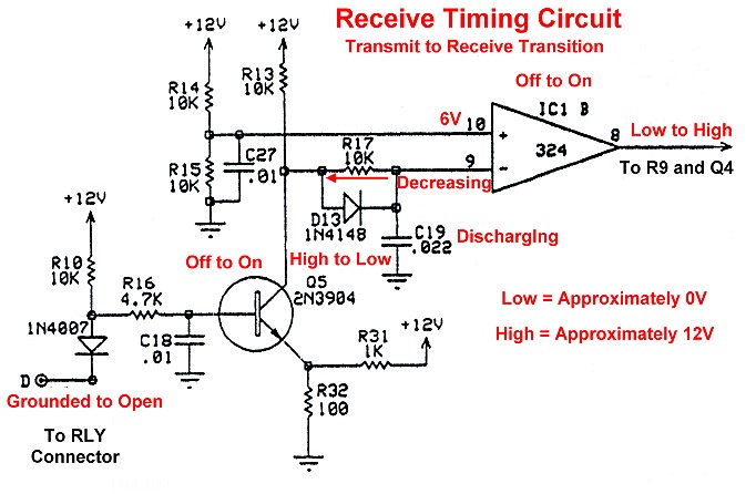
Receive to Transmit Transition:
When the T/R input is brought "Low" to place the QSK-5 in transmit
mode, the current into the base of Q5 is shorted to ground, turning off Q5,
causing the collector of Q5 to go "High". When the collector of Q5
goes high, capacitor C19 charges very quickly through diode D13, which is
forward biased, effectively bypassing resistor R17, as shown by the arrow in
the diagram below. As soon as the potential across C19 exceeds 6V, op-amp IC1B
is shut off, and its output goes "Low". This turns off the receive
PIN Switch. All of this happens very quickly, so that the receive PIN
Switch is shut off immediately when the T/R input is brought low. This gives
the timing circuit a "Fast Off" characteristic.

Receive Timing Circuit During Receive to Transmit Transition
Transmit Mode:
When the T/R input D is grounded, no current flows into the base of transistor
Q5, and Q5 is turned off. The collector of Q5 is then "High", and
capacitor C19 is charged through diode D13. This brings the "-" input
of the op-amp IC1B, to a "High" state. Op-amp IC1B functions as a
comparator. When the "-" input is higher than the "+"
input, as it is in this case, the output of the op-amp is turned off and the
output is near ground potential, or "Low". The output of the op-amp
is connected to the input of the receive PIN
Switch driver, turning off the receive PIN Switch.

Receive Timing Circuit in Transmit Mode
Transmit to Receive Transition:
When the time comes to return the QSK-5 to receive mode, the T/R input is
brought "High". This allows current to flow into the base of Q5,
turning it on, and bringing its collector "Low". When this happens,
capacitor C19 discharges. However, since diode D13 is now reverse biased,
C19 must discharge through R17, the 10k resistor, as shown by the arrow
in the diagram below. When the potential across C19 drops below 6V, IC1B turns
on, bring the op-amp output "High", turning on the receive PIN
Switch.
Since C19 must discharge through R17 during this transition, there is a lag
of several ms after the T/R input is brought "High" before the
receive PIN Switch is turned on. This lag is controlled by the values of
resistor R17 and C19. Increasing C19 increases the delay, as does increasing
R17. This provides the delay needed to insure that the transmit switch has
turned completely off before the receive switch is turned on.
Receive Timing Circuit During Transmit to Receive Transition
In summary, it is the action of diode D13, resistor R17, and capacitor C19 that provides provides the delay that insures that the transmit switch has completely shut off before the receive switch is turned on, as mentioned earlier under Important Timing Considerations.
Transmit Timing Circuit:
The transmit timing circuit is connected to the collector of Q5 just like the
receive timing circuit explained above but with the following changes:
1. The "+" and "-" inputs to the op-amp are switched. This
switches the polarity of the input of the op-amp, and likewise the polarity of
the output. This guarantees that the transmit switch is always off when the
receive switch is on and vice-versa.
2. The polarity of the diode across the 10k timing resistor is reversed.
Switching the "+" and "-" inputs to the op-amp not only
changes the polarity of the output of the op-amp, but also causes the delay to
occur before the switch turns off, rather than before it turns on. To
correct this, the polarity of the diode across the 10k timing resistor must
also be reversed. This makes the delay occur in the proper place, before the
switch turns on.
3. The value of the timing capacitor is decreased from 0.022 uf to 0.01 uf.
This reduces the delay time before the transmit switch is turned on to insure
that the transmit switch is fully on before any RF is transmitted through the
switch.
 Back to Dr. Greg Latta's
Electrical Engineering and Amateur Radio Pages
Back to Dr. Greg Latta's
Electrical Engineering and Amateur Radio Pages
 If you have any questions or
comments, you can send E-Mail to Dr. Greg Latta at
glatta@frostburg.edu
If you have any questions or
comments, you can send E-Mail to Dr. Greg Latta at
glatta@frostburg.edu