| Metering Circuit, Grid Input Circuit, and Bias Power Supply
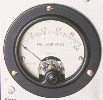
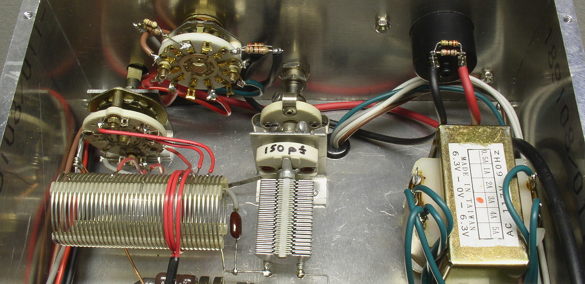
Transformer: The front panel of the amplifier is at the top of the picture in this view of the amplifier. The input band switch and grid inductor can be seen at the lower left in this photo. The input tuning capacitor is in the middle. The meter switch can be seen at the top left, and the meter itself is at the top right. The bias power transformer is at the bottom right in this photo. The bias power transformer is actually a filament transformer run in reverse. Some of the 6.3 V AC from the main power transformer filament winding as stepped back up to 117 V by this transformer to power the bias circuits. |
 Click on the image for a larger view. Click here for a super detailed view. |
| Meter Switch and Grid Input Circuit: The meter switch, which is at top-center in this photo, switches the front panel meter to read plate, screen, or grid current. Because full plate voltage is present on the switch, every other position on the switch is used, providing additional separation between the various metering circuits. The meter and metering circuits were carefully calibrated to be accurate within about 1%-2%. Standard resistors wired in parallel were used to obtain the precise values needed for such accuracy. The input circuit band switch, inductor, and tuning capacitor are also visible in this photo. The grid tuning capacitor floats above ground, and must be mounted so that the rotor plates are not grounded. This requires the use of an insulated coupling on the tuning shaft, as can be seen in the photo. |
 Click on the image for a larger view. Click here for a super detailed view. |
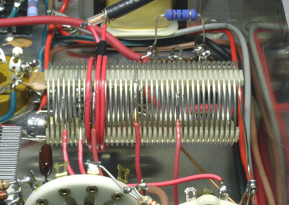
| Grid Inductor and Grid Input Link: In this close-up up the input circuit (grid) inductor, the various taps for each band can be seen soldered to the inductor. The input band switch is at the lower left in the photo, and the input link can be seen wound around the left end of the coil. Click here for information on the location of the taps and construction of the grid input coils. |
 Click on the image for a larger view. Click here for a super detailed view. |
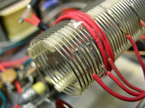
| Grid Input Link Close-Up: Power is fed into the amplifier via a 3 turn link of insulated hook-up wire wound near the grid end of the input inductor. A small amount of epoxy glue (at the top of the link in the photo) is placed over the link to fix it in place. This picture also gives you a good view of the taps on the coil. Taps are made by using a Dremel rotary tool to grind a flat spot on the coil at the appropriate tap point. The tap wire (solid conductor) is then flattened with a pair of needle nose pliers and soldered onto the flat on the coil. Click here for information on the location of the taps and construction of the grid input coils. |
Click on the image for a larger view. Click here for a super detailed view. |
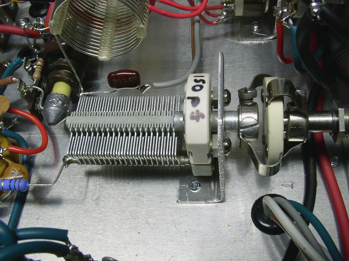
| Grid Tuning Capacitor: The input tuning capacitor tunes the grid circuit to resonance. Because both ends of the capacitor are above ground, the capacitor must be insulated from the chassis. As can be seen in this photo, the capacitor is mounted on an "L" shaped metal bracket and connected to the shaft through an insulated coupling. (If an insulated coupling cannot be found, use a regular coupling with a plastic shaft.) |
 Click on the image for a larger view. Click here for a super detailed view. |
| Amplifier Tube Socket Wiring: Many different things are visible in this picture of the 6146B socket. At the lower left the screen power supply filter choke is just visible. The input circuit coil and capacitor are visible at the top of the picture, the terminal strip in the center of the picture holds the grid bias RF choke and grid current metering resistor, and small terminal strip at the left in the picture holds the plate current metering resistor. The screen current metering resistor (with red band) is barely visible at the bottom of the picture, just to the right of the screen power supply choke. The insulated shaft of the neutralizing capacitor, which pokes through from the other side of the chassis, is visible near the center of the picture. Connection is made to the grid side of the neutrazing capacitor through a grommeted hole in the chassis, visible just to the left of the neutralizing capacitor shaft. |
 Click on the image for a larger view. Click here for a super detailed view. |
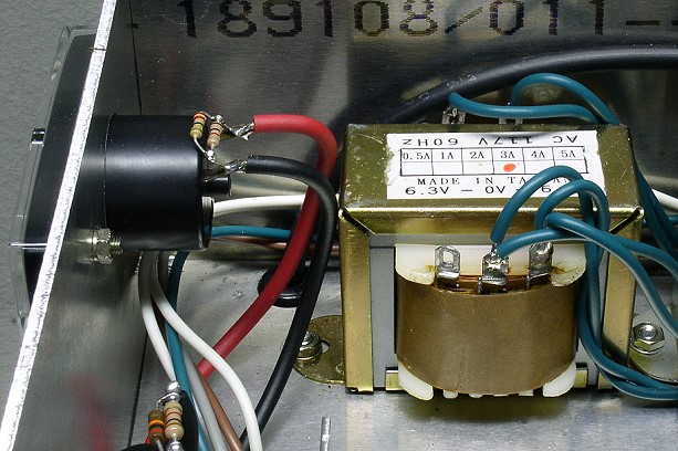
| Front Panel Meter and Bias Power Supply Transformer: In this photo, the front panel is on the left. The front panel meter can be seen at the left, and the bias power supply transformer is visible on the right. The meter shunt consists of two resistors in parallel soldered directly across the meter terminals. Resistor values were chosen so that the metering circuits are accurate to within 1-2%. The bias power supply transformer is actually a 3A 12 V CT filament transformer run in reverse. A 6.3 V transformer would have worked, but I happened to have a surplus 12 V transfomer on hand, so that's what I used. The 3A current requirement is conservative. A 1A or 2A transformer should work just as well. Some of the 6.3 V filament power is fed into one of the 6.3 V windings of the transformer and stepped back up to 117 V. This is then rectified, filtered, and regulated to provide the amplifier bias. Using a standard filament transformer in this manner rather than an expensive and hard to find isolation transformer greatly lowers the cost. |
 Click on the image for a larger view. Click here for a super detailed view. |
| Bias Power Supply Transformer and Plate Power Supply
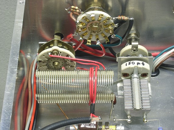
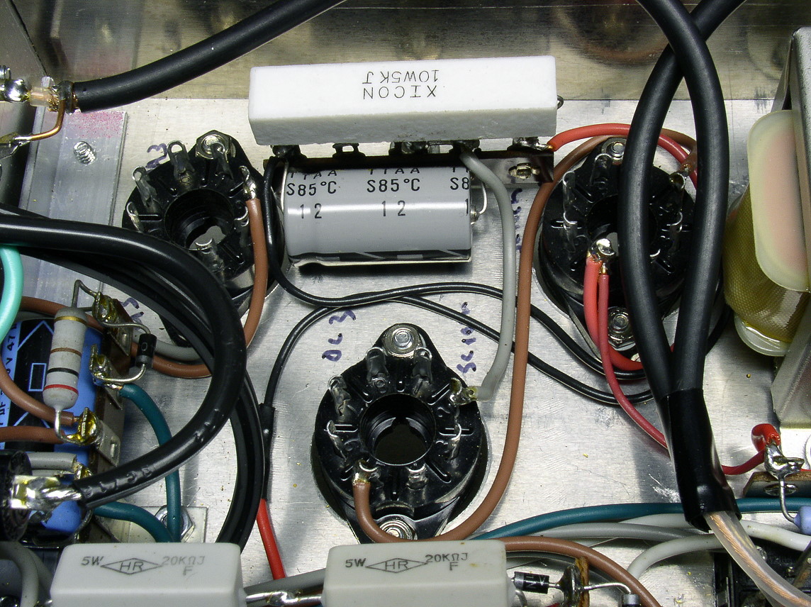
Choke: Many different items are visible in this picture of the middle section of the amplifier. Since signal quality was a top priority in the amplifier, the power supply features filter chokes in both the plate and screen supplies. The plate power supply choke is visible in the top center of the picture, and the screen power supply choke is at the bottom right. The plate supply fillter capacitors and bleeder resistors are just visible at top right. The plate supply rectifiers are mounted on a terminal strip sandwiched in between the plate supply choke and the filter capacitors. Other components visible in this picture are the input circuit is at the lower left and the 6146B socket in the center of the picture. Just to the right of the tube socket is the relay socket and associated wiring. |
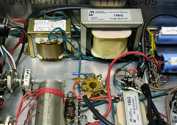 Click on the image for a larger view. Click here for a super detailed view. |
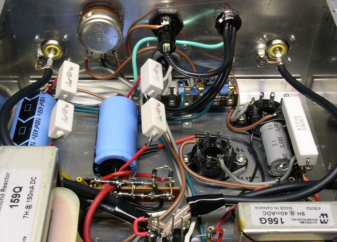
| Back Panel and Power Supply Circuits: The power supply for the amplifier is of the highest quality. Filter chokes are used in the plate and screen supplies, and the bias and screen supplies are voltage regulated using gaseous regulator tubes. The filter chokes for the plate and screen supplies are visible on the left and right respectively at the bottom of the photo. The plate bridge rectifier is visible at bottom center, and the plate filter capacitors (blue) and bleeder resistors (white) are at left and middle center. The screen supply filter capacitor (gray) and beeder resistor (white) are visible at right center. Moving from left to right across the back panel are the output jack, bias control, fuse and control connector, line cord, and input jack. |

Click on the image for a larger view. Click here for a super detailed view. |
| Plate Supply Filter Capacitors and Bleeder Resistors:
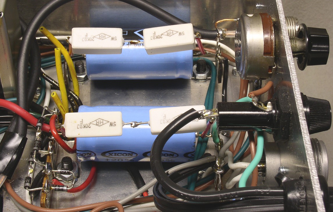
The 6146B amplifier plate supply uses a full wave bridge rectifier. Each leg of the bridge consists of two 1N4007 diodes in series. In this picture near the back of the amplifier the rectifiers are mounted on a terminal strip at the lower left. The bleeder resistors (white in the photo) are two two 20k ohm 5 Watt resistors connected in series across each of the filter capacitors. The two 100 uf filter capacitors are then placed in series. The result is effectively a 50 uf filter capacitor with an 80k ohm 20 Watt bleeder resistor. The back panel is to the right in the picture. From top to bottom on the right are the bias control, fuse, control connector, and line cord. |
 Click on the image for a larger view. Click here for a super detailed view. |
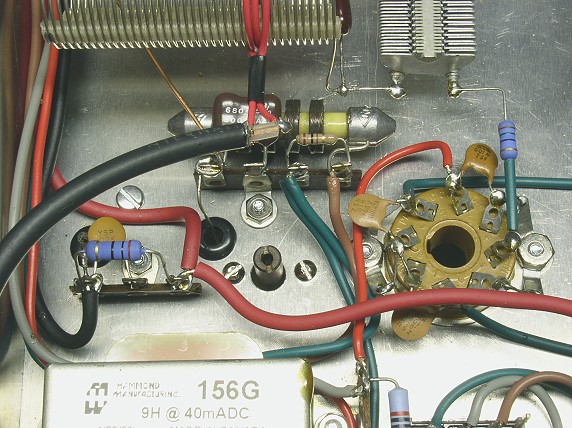
| Voltage Regulator Circuits: The bias and screen power supplies feature voltage regulation using gaseous regulator tubes. The bias supply uses one tube and the screen supply uses two tubes in series. The octal sockets for the these tubes form a triangle is this picture. The bias supply uses a simple half wave rectifier and filter capacitor. These are mounted on a terminal strip visible at the lower left in the picture. The screen supply uses the center tap of the plate transformer as a source of unfiltered DC. This then passes to a choke input filter to the regulator tubes. The filter choke is barely visible on the right in the picture, and the filter capacitor (gray) and regulator dropping resistor (white) are visible at the top in the picture. |
 Click on the image for a larger view. Click here for a super detailed view. |
| Bridge Rectifier and Relay: The plate power supply uses a full wave bridge rectifier. Each leg of the bridge uses two 1N4007 rectifiers in series. Two rectifiers are needed to obtain the required PIV rating. Since the forward and back resistances of modern silicon rectifiers are well matched, balancing resistors and capacitors across each rectifier are not necessary. The rectifiers can be seen mounted on a terminal strip at the top in the picture. The relay in the amplifier is activated when the amplifier is switched from standby mode to operate mode. In standby, the relay connects the input jack to the output jack, bypassing the amplifer. The relay also opens the ground lead on the bias control so that full bias is apllied to the tube, cutting off the plate current. In operate mode, the relay grounds the bias control applying operating bias to the amplifier, and connects the input and output jacks to the input and output of the amplifier. The relay socket is visible at the bottom of the picture. |
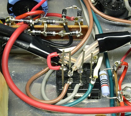 Click on the image for a larger view. Click here for a super detailed view. |
 Back to Dr. Greg Latta's
Electrical Engineering and Amateur Radio Pages
Back to Dr. Greg Latta's
Electrical Engineering and Amateur Radio Pages
 If you have any questions or
comments, you can send E-Mail to Dr. Greg Latta at
glatta@frostburg.edu
If you have any questions or
comments, you can send E-Mail to Dr. Greg Latta at
glatta@frostburg.edu
This page is under constant revision. Please check back often.