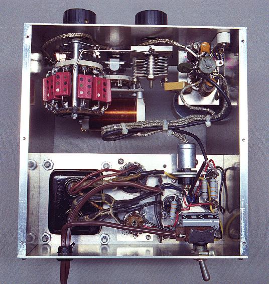
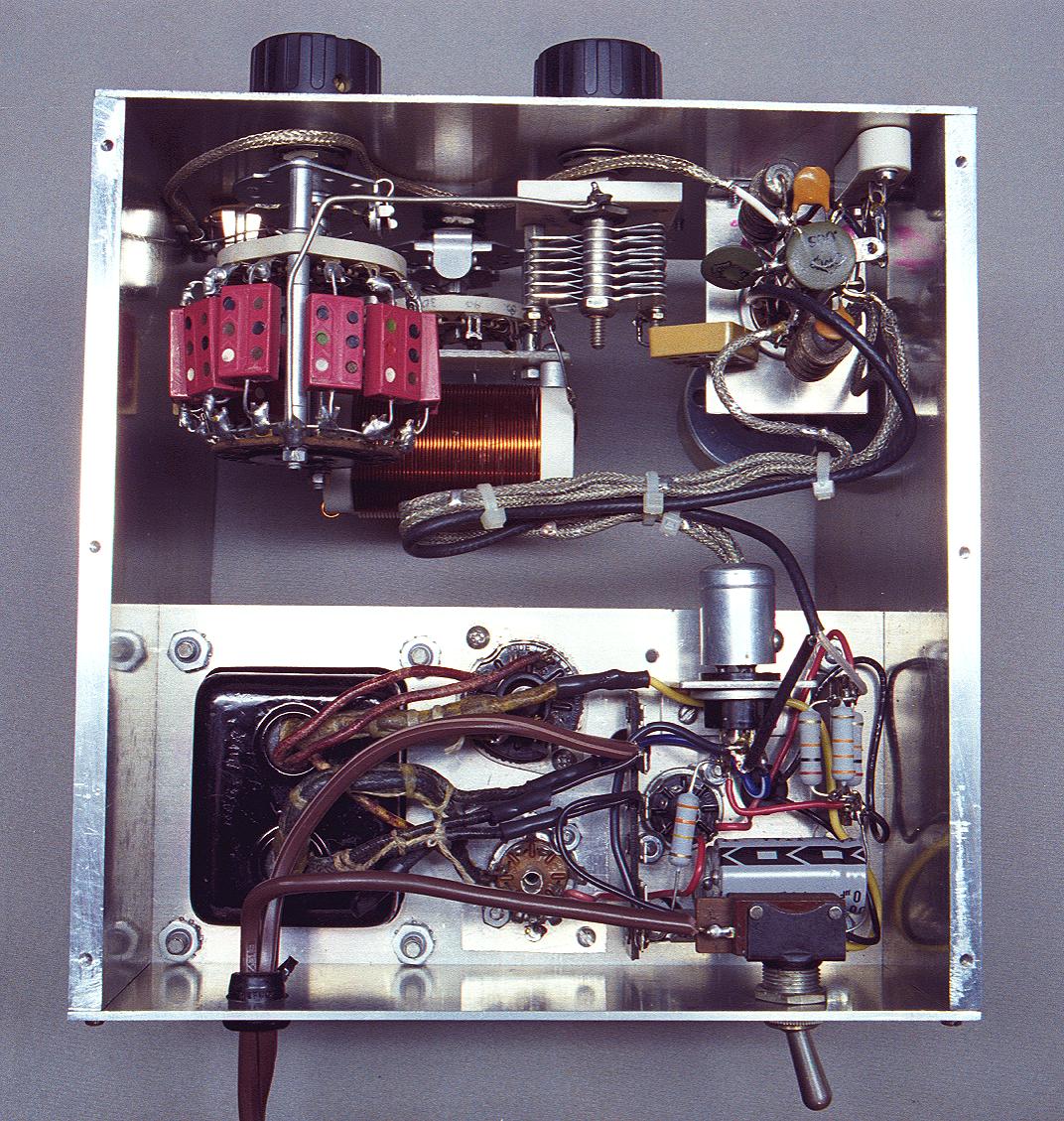
| Complete Bottom View: In this complete bottom view of the transmitter the RF components occupy the top half of the picture and the power supply components occupy the bottom half. At the upper left is the loading capacitor switch assembly (red), at the upper right is the oscillator sub-chassis (green capacitor in the middle), at the lower left is the power transformer, and at the lower right is the filter section of the power supply. See the photos below for more details. |
Click on the image for a larger view. Click here for a super detailed view. |
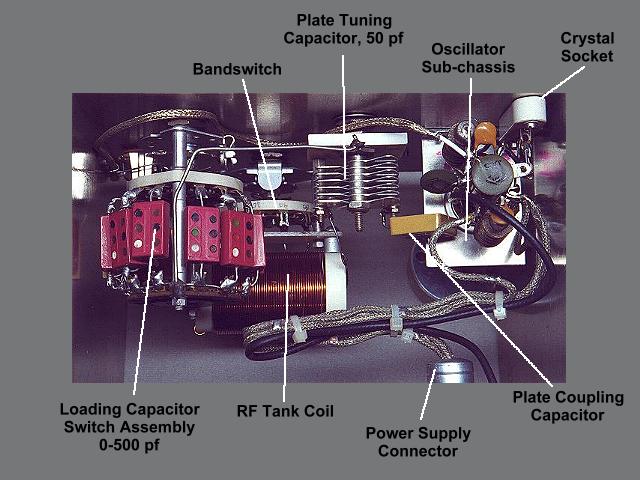
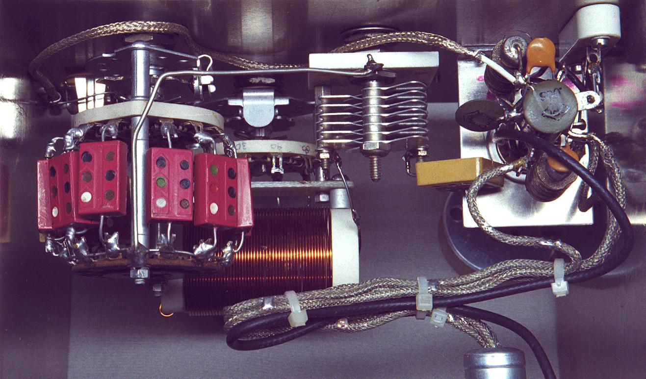
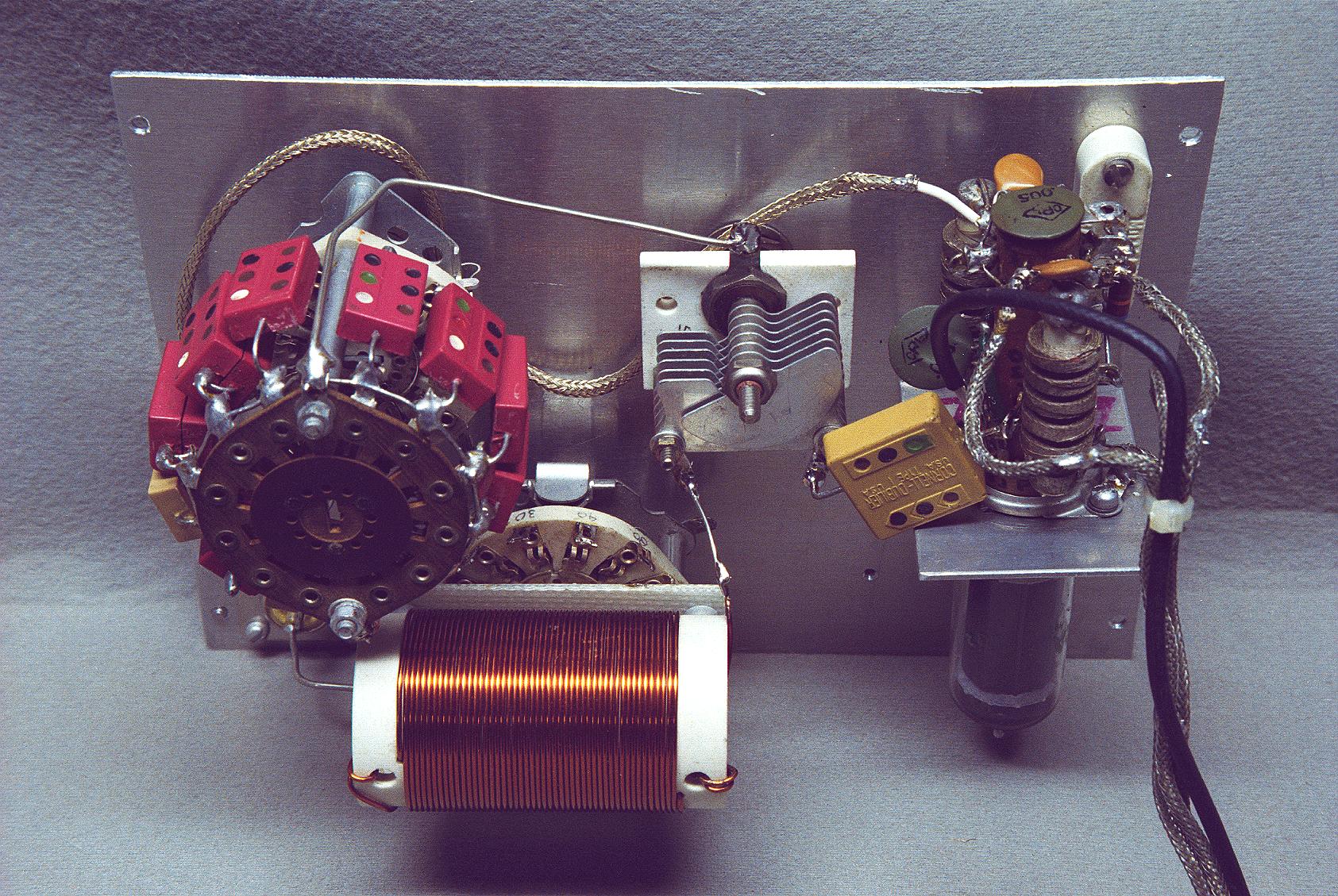
| Bottom View - RF Components: This photo is a close-up of the RF components. Most of this section was built by Jim Trutko, W8EXI.The assembly of red "postage stamp" capacitors at the left is the loading capacitor switch assembly. Rather than use a variable capacitor, Jim chose to use switched fixed capacitors. This is a very nice, though unnecessary, touch. Just to the left of center is the RF tank coil. This consists of heavy enameled copper wire wound on a ceramic form, tapped for each band. The variable capacitor just to the right of center is the 50 pf plate tuning capacitor, and at the far right is the oscillator sub-chassis that holds the 6CL6 tube and most of the oscillator components. The silver colored power supply connector is partly visible at the bottom right. |
 Click on the image for a larger view. Click here for a super detailed view. |
| Bottom View Labeled - RF Components: This is the same as the previous photo but with the various components labeled for easy identification. |
 Click on the image for a larger view. |
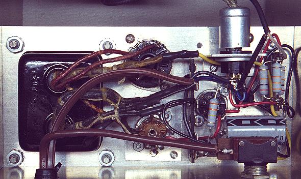
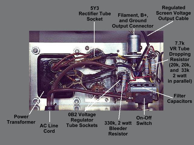
| Bottom View - Power Supply
Components: Though Jim Trutko, W8EXI built most of the RF portion of the transmitter, the power supply was built by me, Greg Latta, AA8V. In this photo the power transformer is visible at the left. In the middle of the photo the large octal tube socket is for the 5Y3 rectifier, and the smaller 7-pin sockets are for the two 0B2 voltage regulator tubes. At the bottom right right are the filter capacitors and on-off switch. At middle right are the 330K bleeder resistor (orange-orange-yellow) and the 7.7K voltage regulator dropping resistor, which consists of three resistors, 33K (orange-orange-orange), 20K (red-black-orange), and 20K (red-black-orange), in parallel. The output connector, which carries B+, filament, and ground to the RF components, is at the top right of the photo. The regulated screen voltage is carried to the RF components by the black shielded cable at the far top right. |
 Click on the image for a larger view. Click here for a super detailed view. |
| Bottom View Labeled- Power Supply Components: This is the same as the previous photo but with the various components labeled for easy identification. |
 Click on the image for a larger view. |
| Front Panel - Interior View: The real guts of the transmitter are all mounted on the front panel. All of the components except the output tank circuit (pi-network) are mounted on a "turret" that is attached directly to the tube socket, just visible below the tube at the lower left. The tube and tube socket/turret are mounted on a small sub-chassis that is attached to the front panel. The yellow "postage stamp" capacitor just to the right of the sub-chassis connects the oscillator to plate tuning capacitor and the output tank circuit. The bandswitch and tank coil are visible near the middle of the picture, and at lower right is the loading capacitor switch assembly. The 1/4" key jack is visible at middle right and the SO-239 output connector is at the top right. |
 Click on the image for a larger view. Click here for a super detailed view. |
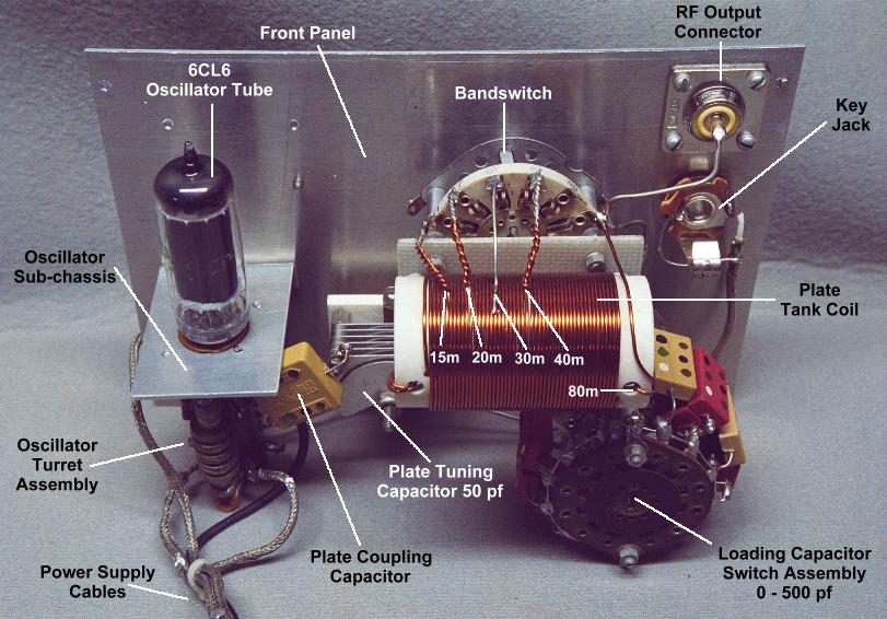
| Front Panel - Interior View -
Labeled: This is the same as the previous photo but with the various components labeled for easy identification. |
 Click on the image for a larger view. |
| Front Panel - Interior View - Inverted: In this upside down view of the front panel all of the important components of the transmitter (except the power supply) are clearly visible. At the upper left if is the loading capacitor switch assembly, and at the upper right is the oscillator turret assembly, which is attached directly to the tube socket and holds most of the oscillator components. The tube is visible directly below the turret assembly. The large yellow postage stamp capacitor is the plate RF coupling/DC blocking capacitor. The bandswitch and RF tank coil are visible at the lower left, and the small variable capacitor in the middle of the photo is the plate tuning capacitor. |
 Click on the image for a larger view. Click here for a super detailed view. |
| Front Panel - Interior View - Inverted - Labeled: This is the same as the previous photo but with the various components labeled for easy identification. |
 Click on the image for a larger view. |
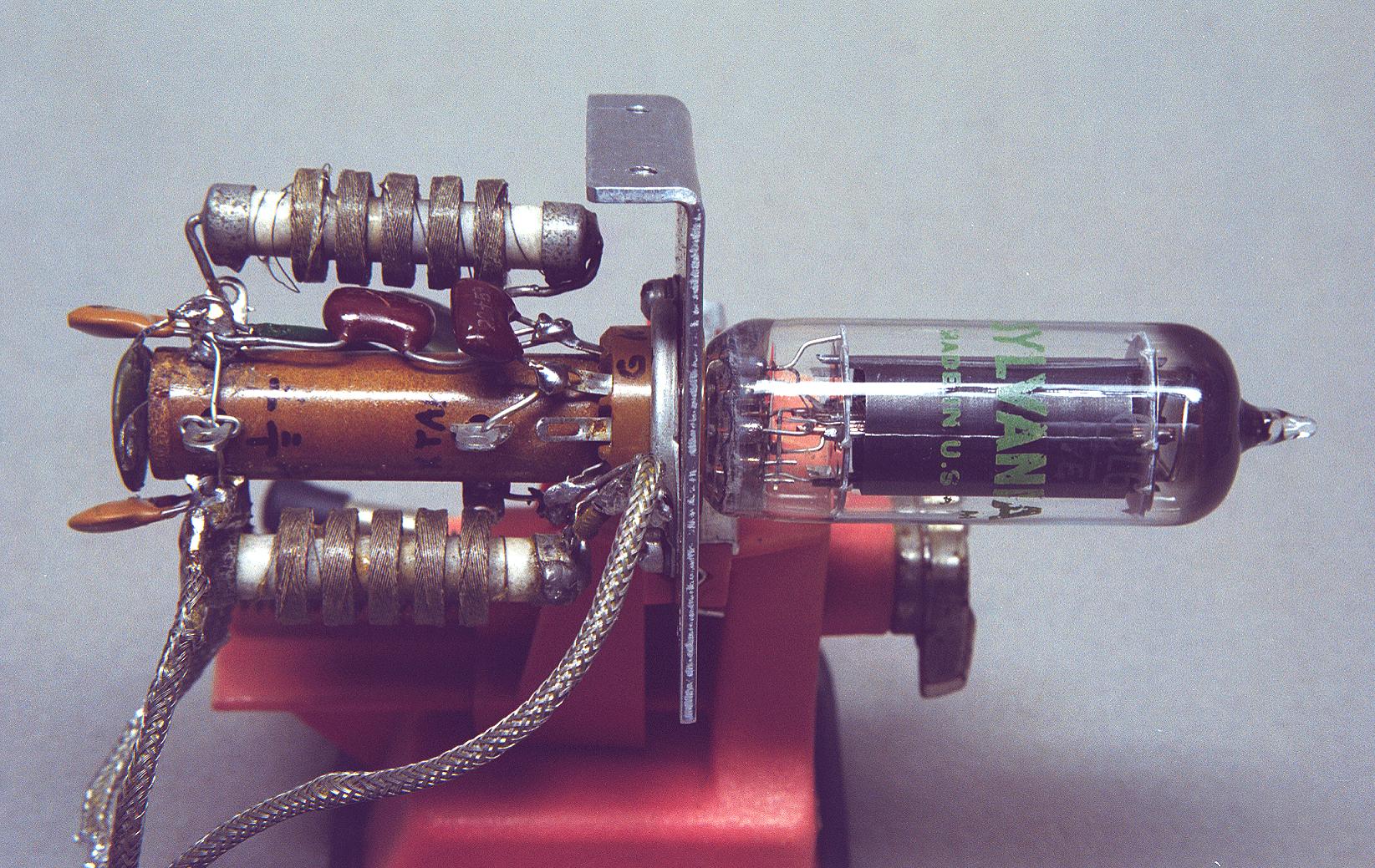
| Turret Assembly: All of the oscillator components (except for the power supply and final tank circuit) are mounted on a single turret assembly that is integrated with the tube socket. Normally used for circuits in early vacuum tube computers, turrets are rarely used in amateur radio equipment, and this is the only one I have ever seen. This circuit was largely rewired, and the original feedback capacitors were replaced with different values. (These are the red molded silver mica capacitors on top of the turret.) The cathode RF choke can be seen at the top and the plate RF choke is on the bottom. The shielded wires carry filament voltage, regulated screen voltage, and plate voltage to the oscillator. |
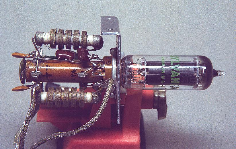 Click on the image for a larger view. Click here for a super detailed view. |
 Click here for pictures and information on the Wingfoot
VFO 2E26 Exciter
Click here for pictures and information on the Wingfoot
VFO 2E26 Exciter Click here for pictures and information on the Wingfoot
813 Amplifier
Click here for pictures and information on the Wingfoot
813 Amplifier Back to Dr.
Greg Latta's Electrical Engineering and Amateur Radio Pages
Back to Dr.
Greg Latta's Electrical Engineering and Amateur Radio Pages
 If you have any questions or
comments, you can send E-Mail to Dr. Greg Latta at
glatta@frostburg.edu
If you have any questions or
comments, you can send E-Mail to Dr. Greg Latta at
glatta@frostburg.edu
This page is under constant revision. Please check back often.